Introduction
This laboratory mainly supports the teaching and research of practical courses related to optoelectronic thin film materials, including various optoelectronic material thin film process equipment (ion sputtering, atmospheric pressure plasma system...) and optoelectronic quality testing instruments.
| Item | Instrument | Function description | Picture |
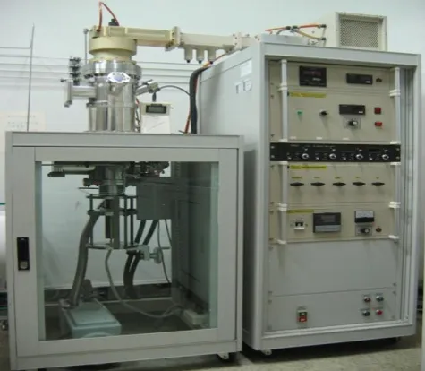
| 1 | Reactive ion sputtering machine (customized) |
Use plasma ions to bombard the target to perform physical vapor deposition. Can deposit metal and ceramic oxide thin film materials. Substrates can be heated up to 500°C simultaneously. | 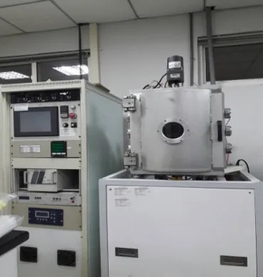 |
| 2 | Rapid temperature rise annealing system MILA-5000 (ULVAC) (Made in Japan) |
Can carry out heat treatment of film test pieces. Heating rate: fastest 50°C/sec. The maximum annealing temperature reaches 1000°C. Annealing atmosphere: nitrogen, argon, oxygen or vacuum (10-5 Torr). |
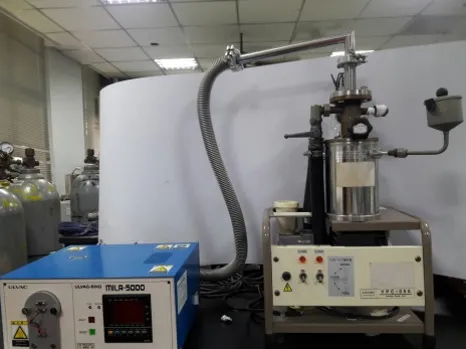 |
| 3 | Reactive RF magnetron sputtering system (Made in Taiwan) |
Using radio frequency plasma to bombard ceramic targets, the main growth materials include functional oxide films such as cuprous oxide, molybdenum dioxide, titanium dioxide, lanthanum lithium titanium oxide, and zinc oxide. | 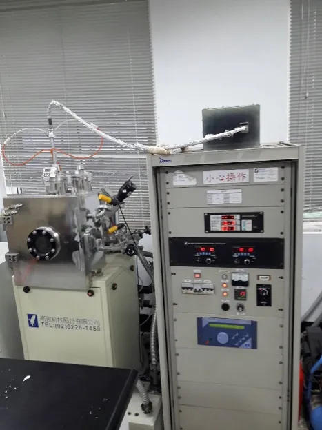 |
| 4 | Hall effect measuring instrument AHM-800B (Advance design technology) (Made in Taiwan) |
Measure electrical properties of semiconductor thin films: Semiconductor type, sheet resistance, carrier concentration, carrier mobility and I-V curve can be defined. | 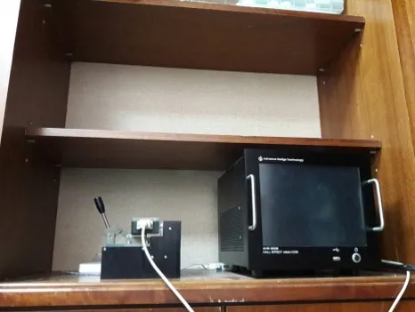 |
| 5 | Sunlight Simulator (XES-40S2-CE AAA) |
Used to measure the true power conversion efficiency of solar cells under different sunlight intensity conditions. Various performance parameters in the I-V curve: open circuit voltage (Voc), short circuit current (Isc), maximum output power (Pmp ), and automatically calculate fill factor and solar cell efficiency. | 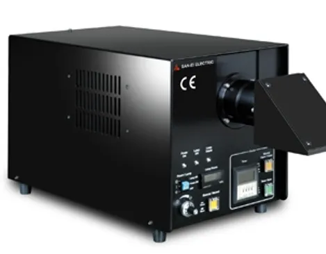 |
| 6 | Sol-gel spin plating machine | Laurell sol-gel spin plating machine uses chemical solution to spin-plate on the substrate to form a thin film. It can be plated with multiple layers and then annealed to improve the density and properties of the thin film. | 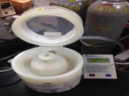 |
| 7 | Large-scale Atmospheric Pressure Plasma Treatment System (Large-scale Atmospheric Pressure Plasma Treatment System) (Made in Taiwan) |
Mainly used in material surface treatment, including (1) surface cleaning/modification, such as display factory: Array, C/F, Cell, Module segment; IC packaging factory/IC testing factory: Die bond , Wire bond, Molding pre-processing; mobile phone factory: EMI coating pre-processing; printed circuit board factory/main board factory/packaging substrate factory: pre-pressing and assembly pre-processing; pharmaceutical factory: sterilization, laminating transfer and printing of drugs and medical equipment Assembly; Plastic products factory: Increase wettability and adhesion, simplify the bonding process; Home appliance industry: Activate product surface, directly join, reduce processing steps; Packaging industry: Activate product surface, increase lamination transfer adhesion; Automobile industry: Strengthen car lamp cover assembly, pre-coating and related adhesion pre-treatment, etc. (2) Surface etching, such as IC semiconductor factory: photoresist removal; printed circuit board factory/mainboard factory/packaging substrate factory: polymer film removal, etc. (3) Surface coating, such as barrier film, anti-scratch film, anti-fouling hydrophobic film, hydrophilic film, photoelectric functional film layer, etc. | 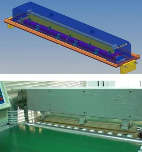 |
| 8 | Microwave Plasma Enhanced Chemical Vapor Deposition System (Microwave Plasma Enhanced Chemical Vapor Deposition System, MPCVD) |
Mainly used in material surface treatment, including (1) surface cleaning/modification, (2) surface etching, (3) surface coating, etc. Advantages of microwave (2.45GHz) as a power supply for generating plasma: The density of plasma generated by RF (radio frequency, 13.56MHz), AC, and DC power supplies is more than 103 times higher >The self-bias is very small and will not cause the substrate or the vacuum chamber itself to heat up or be damaged due to ion bombardment The substrate temperature control device coupled with plasma remote control will enable various High temperature resistant polymer substrate for deposition |
 |
| 9 | Optical interferometer: Laser He-Ne laser Beam splitter Mirrors Photodetector |
Interferometers are commonly used for various optical inspections, such as surface flatness, surface curvature, light source wavelength, light source coherence, material thickness, material refractive index, liquid crystal unit inspection, etc. The installation types of interferometers are quite diverse, and the optical system can be designed according to the detection requirements. | 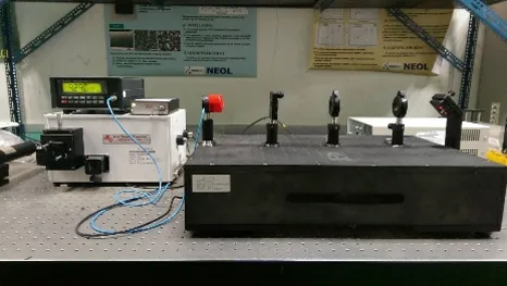 |
| 10 | Light source (Xe-lamp) Monochrometer (ARC SP-308 monochrometer) Infrared light detection system and its accessories (Newport : l: 190 nm-1.1 mm, power measurement range: 0.01mW-2W) |
There are three reflective surfaces scored with different densities inside the monochromater, which are calledFor gratings, the spectrum of incident light can be analyzed by controlling the grating deflection angle and notch. A light source, monophotometer and light detection system can be combined to measure the material's absorption rate of light of various colors. | 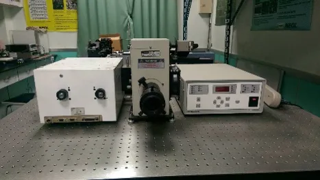 |
| 11 | Four-point probe thin film resistance measuring instrument: electrical measurement meter (Kithley 2700) and four-point probe base. | Resistance measurement is the most basic and important type of electronic material testing. From the measured resistance, the resistivity of the material can be inferred. If the material is a uniform film of known resistivity, its thickness can also be inferred from the measured resistance. Using four probes, using two of them to provide a current path and using the other two to measure the voltage, this method is called four-point probe measurement. This device can be used to measure the radial and axial resistivity of sheet and bulk semiconductor materials, and to measure the sheet resistance (also called sheet resistance) of the diffusion layer. | 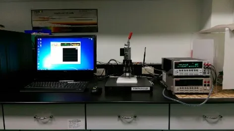 |
| 12 | Polarizing microscope and accessories and image capture system (Olympus, BX51M, Japan) |
The main structure of the polarizing microscope is the same as that of the ordinary optical microscope. The difference is that the polarizing microscope has two more polarizers than the ordinary optical microscope. Polarized light microscopy can be used to observe the crystalline and amorphous states of polymers. In addition, it can also be observed that during the manufacturing process of polymer materials, the arrangement of the internal molecules of the material changes from the original chaotic arrangement to some regular arrangements due to the application of force, resulting in changes in optical properties, which in turn causes polarized light to interfere on the polarizer. When you see the gorgeous colorful patterns, you can get a glimpse of the residual stress distribution during the original production process through these colored interference fringes. | 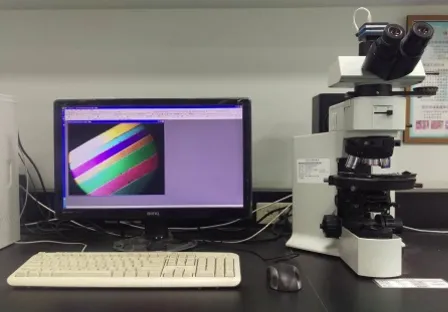 |
| 13 | Ultrasonic atomization assisted chemical vapor deposition system | The precursor solution is atomized with ultra-high frequency ultrasound (2.54 MHz), and then transported into the tube furnace through carrier gas to perform chemical vapor deposition of different optoelectronic semiconductor oxide films. Main growth materials: ZnO, Zn1-xMgxO, Ga2O3, Fe2O3, Co3O4... and other semiconductor oxide films. | 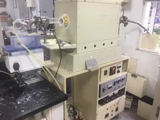 |